![[keith-snook.info]](/stuff/keith-info-S.png)

~ Bicycle Dynamos & RIAA Equalisation Amplifiers ~

Back in the 1970s when I started earning pocket money to buy Vinyl records I had a bicycle that I made from parts of other 'bikes' which I used for my paper round and getting to the main library in the next town
I often rode when it was dark so I fitted a 6 volt dynamo to the rear wheel which powered a red rear light and a dim front light for free ~ No batteries required but also no light when stationary
No matter how fast I rode or spun the wheel with the bike upside–down the lights would not get any brighter and the only way to set the light output was to choose specific wattage 6V bulbs for front and back
Upside-down and spinning the wheel really fast you could get a shock from the dynamo with no bulbs connected ~ The voltage was far higher than 6V but much less than I have experienced since
A bicycle dynamo uses permanent magnets moving relative to a fixed coil of wire to generate a sine wave voltage proportional to the speed of rotation ~ The output from a dynamo is higher than its rated voltage when not loaded but with the correct bulbs attached the light is fairly constant above an initial slow speed because the source impedance is mainly inductive and this impedance increases as the speed or frequency of current increases
Alternators provide fixed voltage for a wide range of speed and load conditions unlike a dynamo ~ They do not use magnets but have 'field windings' fed by direct current to create a variable magnetic field ~ A voltage feedback regulator changes the field winding current to control the output voltage independent of rotation speed or load

Pictured is a commonly used 'schematic' of a bicycle dynamo with 2 bulbs ~ LD is the inductance of the fixed iron cored coil and is also the source of a.c. voltage ~ RD is the d.c. resistance of the coil winding ~ The ratio of LD reactance to RD resistance is large so the impedance Z between b and chassis is referred to as 'mainly inductive'
The dynamo impedance Z is the reactance XL of the inductance LD added to the resistance RD ~ Reactance is the opposition to a rate of change of current through an inductor or capacitor ~ No other components exhibit reactance but all will have an impedance due to elements of L or C like the dynamo or a wire wound resistor
An ideal dynamo has only a fixed coil of wire and a rotating 'permanent' magnet generating a.c. but the coiled wire has inductance LD and also a resistance RD and due to the winding layers has capacitance across it ~ Knowing the total impedance of what's inside will be useful when analysing the dynamo looking into point b relative to chassis
 The schematic above is often used to demonstrate dynamos and other a.c. generators and magnetic pickup cartridges but not correctly because a voltage source in series with the inductor will give an output at d.c. and not a voltage proportional to frequency ~ The schematic on the right is more representative of a dynamo or magnetic pick–up cartridge where the inductor LD is also the generator but neither indicate if the magnet is the fixed or moving part

A current source operating from d.c. to a.c. [an infinite number of octaves!] placed across the generator inductor gives a more accurate generator model ~ Here the bulbs are replaced with a single load resistor R and the unavoidable winding capacitance is added across the inductor which is required along with other components when used for magnetic pickup cartridge and magnetic microphone analysis
All permanent magnet generators have a maximum current limit ~ From stationary or zero Hz the voltage developed across LD is now modelled as truly proportional to speed of rotation or frequency ~ As frequency increases there is a point where XL=RD+R and the current in R is √0.5 x the current limit
The current limit is set by physical properties of the generator like the strength and coupling of the magnets and losses in the magnetic path and the coil winding method ~ The frequency where XL=RD+R is also the point where the power in R is half the maximum it can be and is the −3dB frequency referred to when describing frequency and filter responses or more generally Transfer Functions
Standard wirewound resistors have some series inductive reactance XL and also some parallel capacitive reactance XC but they are or should be mainly resistive ~ The reactive parts of a wirewound resistor or LD in the dynamo do not dissipate any power but they do influence the flow of a.c. as frequency changes due to rotation speed change
Reactances XL and XC are measured in ohms Ω and like resistors oppose the flow of current but only alternating current ~ The reactive value of XL increases and that of XC decreases with frequency ~ XL∝ƒ and XC∝1/ƒ and the actual values at any frequency are given by XL = 2πƒL Ω and XC = 1/2πƒC Ω but these Ωs do not dissipate any power

Although the dynamo schematic above using a voltage source does not correctly represent a dynamo or other a.c. generators like microphones and magnetic pick–up cartridges we can treat the circuit as a L↴R potential divider with a series voltage source VIN at its input and the combined RD+Bulbs=R=1Ω as the output load ~ The dynamo inductor LD is now just L with its reactance XL normalised to 1Ω so XL=R
The white trace below represents the current flowing in the 1Ω resistor R in series with inductor L that has reactance XL=1Ω ~ If the fixed frequency were say 1kHz then the inductance must be 1/(2πƒ)=159µH ~ the value 0.159 [1/2π] crops up a lot when 'normalising' reactive circuits ~ A capacitor with 1Ω reactance at 1kHz has a value of 159µF
The white trace also represents the voltage across the 1Ω resistor because the voltage across and the current through a resistor are always in phase ~ 1V peak [Vpk] across the resistor produces 1Apk through it and the real power in the resistor is 1W peak or 0.5W average ~ Use these links to see IR×VR ~ You can almost feel the heat

The current through the inductor is in phase with the resistor current ~ Because they are in series ~ but the voltage across the inductor is 90˚ out of phase
The peak voltage across the inductor occurs at the zero current crossing points where the rate of change of current is maximum ~ When the inductor voltage is maximum its current is zero and vice versa
In the resistor current and voltage are zero 3 times per cycle where no power is generated ~ In the inductor these zeros occur 5 times per cycle ~ But what happens between these 5 zero points ?
Inductors oppose the flow of a.c. by generating a 'back emf' which is maximum at the maximum rate of current change [crossing zero] ~ In a dynamo LD generates a rotating magnetic field opposing the fixed magnet and because of this a dynamo with a constant load cannot produce more power beyond a certain speed simply by turning faster even though the higher speed generates a higher voltage [inside the dynamo]
The formula for back emf is VL=−L(∂I/∂t) when the current through the inductor falls the voltage across it rises and multiplying IL×VL at any time we get the instantaneous power in the inductor ~ Power [or I×V] is generated between the 5 zero crossing points but unlike the resistors real power half of it is negative [generated by the inductor itself] so the average power per cycle in the inductor is zero but for a part of a cycle could be very real
If an inductor circuit is suddenly broken ~ especially when the current is at a peak ~ the rate of change of current falling to zero will be much greater than at the sine wave zero crossing points ~ Often so great that VL=−L(∂I/∂t) now produces a back emf greater than the normal peak voltage and we may see [or feel or hear] an arc at the disconnection point
If the resistive power is real the inductive or any reactive power ~ half of which is negative ~ can be considered as apparent or imaginary ~ The current through a capacitor is also 90˚ out of phase with the voltage across it and there are also 5 zero crossings and imaginary reactive power when IC×VC is integrated over a whole number of cycles
An ideal inductor will only have inductance no resistance or capacitance ~ Capacitors can be manufactured more ideal than inductors with very low losses and high insulation resistance ~ Practical inductors will have winding resistance and capacitance plus losses due to magnetic field leakage and or hysteresis if cores are used
Inductors change their [not desired] resistance and their [required] inductance as temperature changes ~ They are susceptible to magnetic fields and electro-magnetic fields [EM or Radio waves] and require special housing if used in low signal level and audio circuits ~ Capacitors can use the outside foil of winding as a screen
At any frequency down to zero Hz [d.c.] an ideal reactance will not dissipate any power ~ This condition of zero power despite current flowing only occurs when the voltage across and current through a component are 90˚ apart and that component will be an ideal [never a real or practical] inductor or capacitor both of which can never be ideal but may come close
Any deviation from an ideal reactance can be accounted for by including additional capacitance or inductance or resistance in the component model ~ Dielectric and other losses in a capacitor can be represented by series and or parallel resistors and sometimes by additional C–R paths to model the effect of losses with frequency or time
The proportionally higher losses in inductors can also be represented by series and parallel resistors ~ The core material where used may have non linear losses due to hysteresis and saturation as flux density changes ~ The coil winding resistance is an obvious loss which also increases with temperature and with frequency due to skin effect

The L↴R potential divider circuit normalised to 1Ω described above or a dynamo or a magnetic pickup can be expressed on a graph where the relationship between R and L and Z is easier to envisage ~ This graph is known as an impedance diagram
L and R are in series so the x axis indicates the value of R or the voltage across R as well as the current in the circuit ~ The y axis shows that the inductive reactance or the voltage across L is leading the current through L by 90˚ as in the waveform graph above
We can calculate the voltage VIN across the series circuit and the impedance of the circuit ~ In order to have VL leading VR by 90˚ VIN must lead VR by 45˚ and lag VL by 45˚ in this case where R and XL are the same ~ The magnitude of the impedance |Z| is given by √R2+XL2 and Z=|Z|∡Θ
The impedance Z has to be expressed using 2 terms Magnitude and Phase so Z = 1.414Ω ∡45˚ ~ Applying VIN = 1.414Vpk at the frequency where XL =1Ω the input current will be 1Apk and the circuit waveform relationships will look like those shown above with VIN leading VR and IR by 45˚ and lagging VL by 45˚
On an impedance diagram XL is strictly a vector XL ∡90˚ and XC would be XC ∡270˚ or XC ∡−90˚ ~ If we want to determine |Z|∡Θ for other frequencies or other values of R and L or C and R this x y representation is easier than drawing waveforms but XL needs to be calculated for each fixed frequency so its use is limited
Moving the XL vector to the right to form a 90˚ triangle and applying some trigonometry|Z|∡Θ can also be described as |Z|CosΘ+|Z|SinΘ which is normally written as |Z|(CosΘ+JSinΘ) and known as the 'rectangular' form of the 'polar' vector |Z|∡Θ where +j or −j indicates which quadrant ~ Single L–R or C–R circuit phase cannot exceed 90˚
An impedance diagram is a specific form of Phasor Diagram where it is usual to show resistive vectors R or VR or IR along the positive x axis as a 0˚ phase reference [because resistor V and I are in phase] and reactive vectors ±90˚ ~ Impedance values Z occupy the space in one of the right-hand side quadrants

The negative x axis indicates a 180˚ phase shift relative to values on the positive x axis ~ We can replace −R by j2R where the symbol j = √−1 which Leonhard Euler called an 'imaginary unit' but he used the symbol i as mathematicians do ~ Imaginary power in reactances could only lead to imaginary units
As we have defined j2;R = R∡180˚ it is reasonable to define XL∡90˚ as jXL from which it follows that XC∡−90˚ is defined as −jXC as shown if you click here
The term jXL means that XL is multiplied by j and −jXC that XC is multiplied by −j or j³ ~ Although j is an imaginary concept accept that each multiplication by j rotates a vector by 90˚
Above the series L↴R potential divider impedance was calculated as Z=1.414Ω ∡45˚ because XL R and Z follow the sides of a right angle triangle where Z2=XL2+R2 and in polar form |Z|∡Θ can be calculated knowing the relationship between XL and R is orthogonal [90˚] ~ In the expression Z=R+jXL the j indicates this 90˚ relationship
ZL=R1+jXL is an unambiguous form to define a resistor and inductor in series ~ For a capacitor and resistor in series ZC=R2−jXC ~ The terms R1+jXL and R2−jXC are known as complex numbers because they require 2 parts to define both the amplitude and the phase with time or frequency
The complex impedances R1+jXL and R2−jXC can be added together to give the impedance of a series RCL circuit ~ The real R values and the imaginary X values are added separately Z=(R1+R2)+(jXL−jXC) ~ There will be a frequency where jXL =−jXC and the circuit is said to be resonant and the reactances cancel leaving only (R1+R2)
Here the j operator is simply used to indicate multiples of the 90˚ relationship and remind us that XC and XL are resistances that do not dissipate power ~ If a potential divider is made using two identical resistors the output voltage VOUT is 0.5×VIN but if one arm is a reactance equal to R the output is √0.5×VIN
Time is Constant ~ For a while at least

In the formula VL=−L(∂I/∂t) the derivatives ∂ indicate there has to be a rate of change of current I with time t for VL to exist ~ If the inductor were fed with direct current that increased linearly with time the voltage across L would be constant or put another way if there is a constant d.c. voltage across L the current through it must be increasing linearly until limited by say a series resistor and ohms law saves the day

Configured as shown above the initial rate of change of current through the circuit at t0 switch on [t=0] is VIN/R as shown dotted ~ At t0 VL=VIN and ∂I/∂t must be VIN/R/t
As current starts to flow VOUT across R increases which reduces VL and (∂I/∂t) proportionally ~ As time progresses VL approaches zero and VOUT approaches but never reaches VIN
The currents and voltages follow the curves shown and at time interval t1 VOUT is 0.632 of VIN ~ in the time between t1 & t2 VOUT increases 0.632 of its t1 value and from t2 to t3 . . . yeah it's an exponential curve
The natural response of an L↴R circuit to a step change of input is an exponential curve and will be for a long time ~ Differentiating an exponential curve gives the same curve ~ The rate of rate of change of current is the same as the rate of change of current ~ If ∂I/∂t is made to follow the initial t0 rate we can simply use I/t
If the rate of change of current could be kept linear at value VIN/R/t until VOUT=VIN and I limits at the value VIN/R [as shown by the dotted line] the time now taken to reach VIN is known as the LR circuit time constant and is given the Greek letter tau τ which is also know as the exponential time constant where e−1=0.368

The L↴R circuit [L in series with the input and output across R] is a low pass filter which can also be made with a R↴C circuit [R in series with the input and output across C] ~ In both cases the output will be 0.993VIN after 5τ and for most practical purposes when t>5τ VOUT is considered equal to VIN

Configured as shown above the R↴C circuit current at t=0 is VIN/R ~ As the capacitor charges VOUT increases as shown because VR falling reduces the rate of charge current at the rate VR/R/t
The currents and voltages follow the curves shown and at time interval t1 VOUT is 0.632 of VIN ~ Between t1 & t2 VOUT increases 0.632 of its t1 value and from t2 to t3 . . .
If the current were kept constant at VIN/R the capacitor would charge faster as VOUT increases linearly [shown dotted] until VOUT=VIN at time interval 1 which is also the time constant τ for a C–R circuit
The inductor equivalent of the charge Q=It=CV stored in a capacitor is magnetic flux Φ=Vt = IL but unlike a capacitor we cannot simply disconnect an inductor from a circuit without stopping the current and losing Φ often with a large spark and a big bang
[fact not theory]
Rearranging Φ=Vt=IL we get t=IL/V and substituting I/V with 1/R we get t=L/R ~ From the definition above this is the time constant for an L–R circuit so τ = L/R seconds
Similarly for any C–R circuit rearranging Q=It=CV we get t=CV/I and substituting V/I with R we get t=CR and from the definition for the time constant above we have τ = CR seconds
As shown the L↴R and R↴C circuits have the same response to a step change of d.c. input voltage ~ They will also have the same frequency response or transfer function for a.c. provided the time constants are the same ~ The resistor R can be any value and the voltage transfer function [Output/Input] is fully defined by time constants L/R or CR alone
Leonhard Euler who in the 1700s created the concept of √−1 gave it the symbol i but j is often used ~ He also introduced the symbol for π and many others and did mathematical studies of music and sounds but best of all he proved that [in terms used here] |Z|∡Θ = |Z|(CosΘ+JSinΘ) = |Z|ejΘ which neatly links all the above methods and some
Whatever formula is used for the transfer function of C–R or L–R circuits it is assumed the input is from a 0Ω source and the output is loaded by ∞Ω ~ Hence the statement above ~ R can be any value ~ But in practice not too high or too low and often dictated in practical circuits by values of C or L and the source and load impedances
Although the L↴R and R↴C have exactly the same low pass transfer function they appear as different loads to the source and different impedances to the load ~ At d.c. the L↴R circuit is 0Ω from input to output and with our ∞Ω output load the source sees only R as a load ~ the R↴C source sees an open circuit in series with R
There are 2 C–R circuits and 2 L–R circuits giving 2 high pass filter and 2 low pass filter responses ~ these are passive attenuator circuits where the output cannot be more than the input and the transfer function maximum is 1 ~ There are also 4 Parallel combinations of C–R and L–R but they need finite source and or load R to work against
The methods above for describing C–R and L–R circuits can be interchanged and this is the subject of some interesting mathematics Ref.8 which shows other ways of describing and plotting transfer functions but the most useful I think is Laplace's s notation where H(s) precisely describes a transfer function in simple terms with s as the frequency x axis
Knowing the relationship between current and voltage in C–R and L–R networks as frequency changes and accepting the notion of j as an indicator that they have a 90˚ phase difference we can use basic potential divider ohms law to derive mathematical expressions for the 4 series transfer functions using s–notation where x axis s = j2πƒ

Selecting the H(s) links above there are 2 low pass and 2 high pass filters which are fully mathematically defined from ƒ=0Hz to ƒ=∞Hz using only the variable s [ƒ] and constants CR or L/R ~ From the impedance graph above R+jXL or R−jXC is the complex impedance Z looking into each series network and √R2+X2 is the magnitude or real part of Z expressed |Z|
Considering the 2 low pass filters where H(s) = 1/(1+s) and where 1+sτ is derived from R+jXL or R+jXC it follows that 1/√(1+sτ)2 is the ratio of R/|Z| which is VOUT/VIN so we can plot the amplitude response [A] against frequency [ƒ] ~ Phase is the imaginary part of Z and relative to 0Hz is tan-1(X/R) or using s notation the phase of H(s) is tan-1(sτ)
RIAA Equalisation aka BS 1928
The Recording Industry Association of America [RIAA] was formed 1952 to oversee payment of copyright fees for music artists and around 1954 along with other international 'associations' they also set a new fixed definition for the Equalisation required to record sound on the emerging Fine or microgroove gramophone discs
This 1962 Wireless World article Ref.9 has more about transfer functions and leads into explaining Poles and Zeros with an example of a more complex transfer function [Fig.2 p.226] for a Fine Groove Disc play–back equaliser' with 3 time constants ~ The equivalent British Standard BS 1928 or RIAA vinyl record specification
The RIAA or BS1925 replay Equalisation [EQ] combines 2 low pass filter sections of the form 1/(1+sτ) [poles] and 1 section that can only be called the inverse of a low pass filter (1+sτ) [a zero] ~ The 3 individual transfer functions are multiplied like any other numbers to give an accurately defined replay transfer function
.svg)
For each low pass filter section the denominator approaches zero as sτ approaches -1 and H(s) approaches infinity but unless negative frequency exists this cannot happen ~ If the H(s) numerator approaches zero the whole function approaches zero hence the term ~ When graphs tend towards infinity they can look like circus tent poles hence the term
The engineer way to present transfer functions is a graph of amplitude [A] and maybe phase [P] against frequency [ƒ] ~ If the Y axis is in dBs we can easily display several decades of gain or attenuation and making the x axis the log of frequency keeps the graph narrow and clearly shows linear changes like 20dB/decade as straight sloped lines
I try to keep the suffixes of the 3 RIAA time constants τ3 τ2 and τ1 in frequency order with τ3 assigned to the lowest frequency but it can be seen that swapping τ3 and τ1 makes no difference to the result ~ The standard [specification] for Vinyl disc playback or replay and record only has only 3 time constants and is only defined between 20Hz and 20kHz
τ3=3180µs ≈50.05Hz τ2=318µs ≈500.5Hz τ1=75us ≈2122Hz

.svg) Magnetic Cartridge RIAA Replay EQ
Magnetic Cartridge RIAA Replay EQMagnetic Cutter Head RIAA Record EQ
Ceramic Cartridge RIAA replay EQ
The magnetic cartridge RIAA replay graph above shows the amplitude response A in dB against logarithmic frequency for the RIAA curve as defined by its 3 time constants ~ The 3180µs pole corrects from 50Hz upward for the signal from a magnetic pickup which like a lightly loaded dynamo is proportional to frequency
Ceramic and crystal cartridges have an output that is proportional to the the groove amplitude so do not require the 3180µs time constant as I mention here with reference to the QUAD QC22 and its simple EF86 valve phono stage ~ They may still need the other time constants provided by the reduced ceramic cartridge RIAA replay EQ
A magnetic cartridge may be a moving magnet or moving coil or moving iron but whatever type it is when correctly loaded it should have an output that increases at 6dB/octave [6dB/oct] which is the inverse of the slopes of the RIAA Replay graph between 50Hz to 500Hz and 2122Hz to >100kHz although the standard is only defined between 20Hz and 20kHz
Now may be a good time to read Ref.1 at least from p.100 onward
The RIAA Record EQ graph above is also the response of the output from a magnetic cartridge as well as the EQ curve for the voltage to a record cutting lathe that uses a magnetic cutting head which most do although some are piezo and so use an inverse of the Ceramic RIAA EQ curve but however your vinyl records are cut that's what you get
Recording and Playback Velocity and Amplitude
If a level frequency signal is fed to a magnetic cutting head the amplitude of the groove will reduce 6dB/oct due to the cutter impedance increasing proportionally with frequency ~ This makes the maximum velocity of the cutter constant as indicated below by the same slope of the zero crossing point tangents ~ This is referred to as Constant Velocity

With RIAA Record EQ applied the frequencies 50.05Hz to 500.5Hz and 2122Hz to 20kHz to a magnetic cutter will give a constant Amplitude cut because the 6dB/oct fall of the head current is negated by the 6dB/oct rise due to the Record EQ
Below 20Hz and above 20kHz the RIAA standard is not defined and recording studios take precautions to protect their cutter heads and the recording medium ~ sometimes with an additional 12dB/oct reduction above 50kHz on some cutting laths and sometimes modifying the bass response
Cutting head velocity has a 'slew rate' expressed in cm/s which is limited by the mechanics of the head and the mastering material used and which varies from outer to inner tracks due to the change of linear velocity ~ As stated above RIAA Record EQ gives 2 sections of constant amplitude cut either side of the audio band centre
A 12" Long Playing [LP] microgroove disc turning at 33⅓ rpm has a linear velocity of about 0.5m/s [50cm/s] at the outside edge and at a squeeze fits an average 100 grooves/cm when using variable pitch spacing ~ The highest obtainable recorded velocity cannot exceed the linear velocity due to the flat face and 45˚ back angle of the cutting tool

For calculating any slew rate the peak excursion of the signal needs to be known and with ≈100 grooves/cm the cut can swing ≈40µm either side of groove centre ~ Ignoring linear velocity and position on the disc the maximum velocity of recorded audio occurs at 20kHz and can be determined from the diagram shown
The period of one cycle of 20kHz is 2π=50µs so tr=25µs is the duration of a ±40µm excursion ~ 80µm/25µs =5m/s shown dotted is less than the true slew rate but 10x the highest linear velocity so cannot possibly be cut ~ The zero crossing maximum velocity will actually be π/2 times greater at 7.854m/s
Remember the little bend in the RIAA curve around 1kHz it is actually a step of 12.5dB [4.217x] between 50.05Hz to 500.5Hz and 2122Hz to 20kHz as seen in the constant amplitude Ceramic EQ curve so the maximum recorded velocity at 20kHz is reduced to ≈1.86m/s [186cm/s] which still cannot be cut
This 12.5dB step also reduces the dynamic range required for RIAA EQ to 40dB ~ If τ2 and τ1 were not included for either magnetic or ceramic cartridge EQ the 3 decades from 20Hz to 20kHz would require a range of ≈60dB
With the 12.5dB step the maximum lateral velocity at 8kHz is ≈19µm/62.5µs×π/2 =0.477m/s which is just about recordable at the edge of a 12" 33⅓ rpm vinyl record ~ Between 2kHz and 8kHz it is possible to have higher than expected levels without distortion and nowadays with better variable pitch more bass output is possible so we get more even if not required
This is the way gramophone record reproduction is and always has been ~ Unlike CD players and other digital media the gramophone recording process relies on the energy distribution of the music which should be more than 30dB lower at 20kHz than at 1kHz even for music made nowadays and much lower relative to the bass on some recordings
Vinyl test discs like TCS101 [Stereo constant Frequency bands from EMI] have a 0dB reference of 1cm/s rms at 1kHz which would be ≈5cm/s rms at 20kHz but they record tones above 10kHz 6dB lower ~ Commercial test discs like HFS69 use 5cm/s at 1kHz and state for their 300Hz tracking tests figures like +15dB ref. 1.12x10⁻³ cm peak which would be an excursion of 63µm presumably only in one direction due to the wording
What is cut on your vinyl record is what you get ~ It is what the artist and or the producers or cutting engineer decided within the limits of the medium and the technology used at the time ~ It may have been recorded or cut directly with valve equipment or transferred from 4 track tape or processed in the most modern digital studio ~ All we can do is get the replay equalisation and the low noise amplification correct
Here is yet another graph to show the 3 RIAA replay time constants separately or in the combination τ1+ τ2 as used to EQ crystal or ceramic cartridges ~ Click on the links below to select various curves or download as a layered pdf which I made 1997 and may not work in some browsers but should work in acrobat or other compliant pdf readers

RIAA Replay
Gain & Phase
τ3 only
τ1+τ2 only
τ1τ2τ3
RIAA = τ2/τ1τ3
As stated above British Standard BS 1928 aka RIAA precisely defines the EQ for fine or micro groove vinyl records made after 1954 using only 3 time constants ~ It was an agreed world standard until in 1976 an IEC amendment added a 7950µs pole [albeit with a zero Ref.9 p.229] to the replay EQ to effect a high pass filter−3dB at 20Hz to reduce rumble
During the 1970s a.c. coupling was used between phono stage and pre–amp and power amps so several high pass filters already existed in many Hi–Fi systems and in 2009 the 7950µs high pass pole was removed ~ More aggressive rumble filters are often built into phono stages but they should not be considered when calculating replay EQ [Ref.10]
Another 'amendment' that crept into RIAA amplifier folklore due to the late Allen Wright [Ref.6] and some internet wild fires is an additional pole at 3.18µs [50.05kHz] which appears to fit 'numerically' with the other RIAA time constants but is not required as it corrects for an 'incorrect' high frequency roll off for Neumann lath cutter heads
Even if some record cutting lathes have a pole above 20kHz [which most do] attempting to correct for it at replay is both restrictive and difficult and a waste of time ~ The cutting head output falls above 20kHz due to losses and there is often a formal pole somewhere beyond 40kHz which may be 2nd order [12dB/oct] or higher to prevent cutter meltdown
Calculating R & C Values for RIAA Equalisation
In the past Analogue Radio and TV broadcasters placed the complexity of their systems at the studio and transmitter such that consumer receivers could be made easily and repeatable at low cost ~ The reproduction of music was intended to be similar and the equipment for vinyl discs would use only 2 R and 2 C [2CR] for RIAA equalisation
That was the plan and correct application of the chosen replay Time Constants [TC] was not difficult for manufacturers who followed the rules ~ Like QUAD and LEAK and Radford in the UK who had switched EQ for RIAA and earlier discs [and Tape Heads] that used the same input amplifier which was often a single pentode valve
Most early gramophone designs used 2 terminal 2CR Lumped Networks in a Negative Feedback [NFB] Loop around the single valve ~ usually direct from the anode back to the grid ~ with a series input resistor for the required load and gain determined by the network impedance ~ The QUAD QC22 circuit is a good example
Not long after the 1955 publication of the British 'RIAA standard' BS 1928:1955 an article by J. D. Smith appeared in Wireless World [WW] magazine suggesting that the application of 2CR replay EQ ~ which was intended to be simple ~ was being misunderstood and misquoted by Numerous writers and he did the same
In January 1957 W. H. Livy of EMI Studios London replied by letters WW to the article and J. D. Smith responded ~ Later in 1980 when I read the dialogue I agreed with Livy who after-all was making vinyl records and the equipment used ~ It prompted me to calculate the 4th network using 2CR and present the results simpler [ref.11]
In the early 1980s I was working for a small [only 2 TV channels] British broadcaster and had access to a HP85 which could easily 'do the math' and print results which gave three 2 terminal networks by Livy and the 4th 2 terminal 2CR plus the two 4 terminal 2CR networks that can be scaled for any impedance ~ When the HP85 was available
Later in 1986 I was issued a PSION organiser and I rewrote the RIAA programs in OPL in the small 16×2 character display on long bus rides in & out of London ~ I also wrote some engineering utilities and other programs ~ And since 2001 html versions available here with some changes to make choosing components simpler

Probably due to the 1979 IEC amendment a draft paper [Ref.10] by AES member Stanley P. Lipschitz listed a large matrix of RIAA Network+Amplifier topologies rather than just the values required for each Network N which led to further confusion and the my cat's blacker than your cat overindulgences of Margan Self Slee Vogel van de Gevel et alii
Pictured is a section of Lipschitz’s Fig.2(b) or not to be taken too seriously ~ It is formulated around a non specified amplifier using one of the four possible 2 terminal 2CR RIAA networks N [his Fig.1 my Ref.11] but with additional R3 R0 and C0 which introduce the extra pole ω2 and zero ω6
Changing or removing R0 will not affect the RIAA EQ due to N but is not an option with this topology as it puts the cartridge output ei into a virtual earth but then the Lipschitz paper never considers that phono cartridges require specific loading to work correctly ~ For a load of R0 ≈47kΩ the d.c. impedance of N would be 1.5MΩ for a 30dB gain
The resistor R3 does affect the EQ as shown at ω6 and even if not fitted the output impedance of the non specified amplifier will affect the EQ ~ Active RIAA is a passive network spoiled by feedback ~ ω2 due to C0 is included for the IEC amendment 7950µs and this along with the vague zero ω6 was enough for me to question the rest of the document
It is clear Stanley Lipschitz is a mathematician from the Layout and Introduction of the draft paper and his use of X for poles and O for zeros in his diagrams which use piecewise straight lines with no specific scales but we can assume the slopes are 6dB/oct ~ I like this simple presentation and have often used it myself and I appreciate the effort ~ however:
What I don't like about the paper are the Abstract / Introduction which states Most current disc preamplifiers have audibly inaccurate RIAA equalization. . . due in part to the perpetuation in print of incorrect formulae for the design of the RIAA equalization networks but the work by RCA and Livy at EMI and others in the 1950s [ Ref.2 ] is not mentioned
The AES is a closed shop and non members have to pay to see articles published in their journals ~ This is reasonable but greatly restricts expanding knowledge and receiving valid feedback from outside the box about questionable articles and audio innovations so I have to agree with Grouch Marx ~ But luckily not all members agree with each other

The Stanley P. Lipschitz Published paper [Ref.10] lists the QUAD 33 pre–amplifier along with 'Distortion in low–noise amplifiers ~ Eric F. Taylor' WW Aug 1977 among references 19 to 29 which he states are good design and also lists 1 to 18 as those with 3 major errors he defines as:
1) Incorrect design equations for the calculation of resistor and capacitor values ~ Use my online calculators RIAA–1 and RIAA–2 and adjust only the largest resistor to allow for additional impedances either side of or across the RIAA network as the QUAD 33 does ~ Commercial design values are most likely correct apart from the larger value R [does not work well for RIAA–3 and RIAA–4]
2) Failure to take into account the fact that there is an additional high–frequency comer in the response of an equalized non-inverting amplifier stage ~ Don't use this topology or use the inverting amplifier with shunt NFB plus an input buffer and low R values if worried about noise ~ Or better still no networks in a NFB loop [Passive RIAA]
3) Failure to correctly take into account the limited loop gain available from the amplifier circuit ~ Lipshitz's published paper Fig.6 tries to show the effect of inadequate gain and limited high frequency gain due to an integrating open loop gain but fails to show that a simple amplifier with adequate gain can place an impedance across a 2 terminal network in a NFB loop [ref 1) above]
With the introduction of good 'audio' op–amps things did get better and simpler but then followed changes back to valve discrete and balanced amplifiers using valves and transistors and distributed time constants plus additional poles and IEC amendment ~ Keep the RIAA network or sections of it separate from the amplifier gain setting components where possible
Active or Passive RIAA EQ ?
Lumped or distributed Time Constants ?
Op-Amps or Valves or Transistors ?
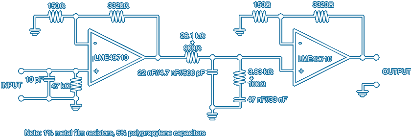
The circuit above is a direct copy from the National Semiconductor now Texas Instruments [TI] data sheet for their Hi–Fi Audio operational amplifiers ~ the low noise low distortion LME49710 and LME49860 etc. and although it is only offered as a typical application it demonstrates how little thought goes into these 'designs'
It does show however how a good modern RIAA EQ amplifier can be made using op-amps with predictable gain and very low output impedance and high input impedance such that a simple 2 Resistor and 2 Capacitor passive RIAA EQ block can be placed between them without any interaction or undue signal loss
It looks like TI have carefully crafted the capacitor and resistor values to provide the most accurate RIAA EQ possible ~ The resistors are chosen from the E96 series and as stated are 1% tolerance but I have seen a TI application that recommends 0.1%! but the capacitor tolerance of 5% puts paid to any precision these circuits offer
26.1kΩ+909Ω =27.009kΩ and 3.83kΩ+100Ω =3.93kΩ so why not use single E24 series 1% values of 27kΩ and 3.9kΩ ? ~ Calculated using 27kΩ the capacitor 47nF∥33nF should be 81nF not 80nF so use 68nF∥13nF or 51nF∥30nF ~ Capacitor 27nF∥4.7nF∥500pF should be 27.769nF so rather than 5% polypropylene why not use 27nF∥750pF 1% polystyrene which are readily available and are better capacitors for this application
The circuit layout below with all 3 RIAA time constants 'lumped' in a passive equalisation block between 2 op-amp stages has been used for so many 'boys own book' and Hi–Fi magazine articles but unfortunately its simplicity is often ruined ~ A good example how not to make a phono pre–amp using this method was published by Hi-Fi World

The RIAA–1 topology using standard E12 values [E24 1% in practice] gives a more accurate RIAA equalisation than the Texas Instruments design which has a peak–peak deviation of 0.16dB using perfect component values ~ The age old standard values of 47k 6k8 16n and 47n have a peak–peak deviation from RIAA of only 0.05dB
This circuits Passive Network RIAA–1 is a higher impedance than the TI circuit but this does not affect the noise performance which is dominated by the source S/N and IC1 R4 R5 noise voltages ~ Both circuits have similar overall d.c. 0Hz gain which is about 500x or a 3mV cartridge input gives an RIAA EQ output of about 150mV
The open loop gain A0 and GBW of the LME49710 enables the gain A of each stage to be increased without affecting the S/N significantly ~ If R4 in my circuit were changed to say 100Ω a 3mV cartridge input would give 320mV output with theoretically better S/N ~ Also changing R6 to 1k would give about 0.7V out for a 3mV input
Both circuits are d.c. coupled which is not desirable for a phono stage but rather than use coupling capacitors which would also require additional resistors for d.c. biasing it is possible to place capacitors in series with R4 or R6 or both ~ The capacitor values should be calculated to provide a high pass response say –3dB at 20Hz or lower
With capacitors in series with both R6 and R4 the final slope of the the high pass response will be 12dB/oct and will provide a reasonable rumble filter that may not be appreciated by some critics even though it keeps the through signal path d.c. coupled and the input offset voltages of the op-amps are now amplified only 1x not >500x

The accuracy of the 2 circuits above was made with PSpice computer modelling using a Laplace Analogue Behavioural Model [ABM] to provide a mathematically perfect inverse RIAA source with a 0Ω output impedance
The circuits were modelled with the load RL as shown in the schematic so the input impedance of the next stage could be accounted for if required
If the amplifier impedances either side of the lumped RIAA block are not zero output and/or infinite input which is what you will find in practice ~ especially when using discrete amplifiers ~ allowance can be made for RL by making the value of R1∥RL the calculated value of R1 as shown here [Valid for 2&4 terminal RIAA–1&2 networks]
The output [source] impedance of the first stage amplifier [Rs] is in series with R1 so can be incorporated into the RIAA network as R1=R1[calculated]–Rs ~ And incorporating RL of the next stage a single new value of R1[calculated]=(R1+Rs)∥RL will give correct EQ for the 4 terminal topologies of RIAA–1 and RIAA–2
My RIAA calculators are useful for quickly checking published phono amplifier designs ~ which despite Ref.2 and the Lipschitz paper and the many expert books still have errors ~ Some expert authors do not give tables or calculations used in their RIAA amplifiers claiming it's 'too complicated to explain' others give 'Novel' copyrighted designs?
Electronics for Vinyl by Douglas Self gives precise component values like 344.7kΩ and 9.132nF for his lumped 'Configuration A' topology [RIAA–3] but then shows circuit Figure 10.11 with R5=1.8MΩ which is more than twice what it should be plus the series NFB means the response requires a 4th gain dependant time constant
Selfs figure 10.11 [online somewhere] is derived from the H. P. Walker circuit [Ref.13] which used RIAA–2 so that R14 sets the 0Hz gain and can be easily adjusted for impedance across the network without upsetting the EQ response but Selfs circuit using RIAA–3 cannot be readily corrected by R5 due to the 0Hz path being via R5 and R6
You may often see RIAA networks with multiple parallel and series components to make 'precise values' that don’t fit the RIAA calculation but have been 'eased' because they are 2 terminal networks in feedback loops where the impedances either side are not suitable and/or cannot be incorporated into the network as RL and Rs above
Aside from problems where the amplifier output impedance is not low enough and negative feedback is developed across say a 1kΩ or greater resistor ~ the use of a 2 terminal RIAA network in a feedback loop means that the gain reduction limits at high frequency at 0dB [1x] often requiring an additional CR correction at the output
For the above reasons and the fact that a high gain amplifier negative feedback network with a 40dB slope just does not sound correct and is often the reason why small scratches on a disc appear 'bigger' than they should is why I prefer passive EQ but if you feel different please do hesitate and do not let me know
One old commercial design that used negative feedback around a 2 transistor amplifier similar to Douglas Self’s and got it right was the QUAD 33 which used a 2 terminal 2CR network [RIAA–2] where the bias resistors form part of the network so R303 & 304 appear as R3=101kΩ for calculation and C103 and 104 are a custom 29nF
While writing these pages I sometimes check to see if the information I intend to add is not available better elsewhere on the internet and I often find some classic misleading and annoying statements like: 'An LCR RIAA network has to be used for passive EQ because the common CR type can only be used in a feedback loop'
It is true that network topologies RIAA–3 & RIAA–4 cannot be used for a passive circuit placed between 2 amplifiers like the TI application above but all 4 RIAA 2CR lumped network topologies can be used in a passive non feedback form if they are used as the load of a 'transconductance' amplifier with very high output impedance

The valve circuit on the left uses the same lumped passive EQ RIAA-1 as my LME49710 circuit above but configured for current drive ~ The output of the ECC81 triode can be considered as a current source with an internal shunt resistance ra of about 31kΩ @ Ia = 1mA
The un-bypassed 1.8kΩ cathode resistor R11 sets the anode current at 1mA and also raises ra to ra' ≈ 126kΩ so the effective resistance of R1 is 126kΩ∥75kΩ which is the required 47kΩ for this RIAA–1 block or a RIAA–2 but is not suitable for RIAA–3 or RIAA–4 ~ See Triode Un-bypassed Cathode
A valve stage configured as shown needs a high input impedance following stage and any load of the next stage like a grid resistor must also be incorporated into the calculation but as the total value of R1 is the only parameter that needs adjustment the calculation is simple and predictable
The network components C1 & C2+R2 would best be connected to ground ~ The un–bypassed R11 makes the triode a better but not perfect current source and may make the stage susceptible to noise induced from the heaters so a pre stage and d.c. heaters might be needed for best S/N depending on the triode used
Using a current source as a valve anode load with all the EQ block returned to ground offers little or no advantage and would introduce semiconductors and additional shot noise ~ Because another stage may be required before the valve EQ stage for best S/N this may lead to the conclusion that separate time constants between gain stages would be simpler?
Several stages are often required to amplify the small signal levels from magnetic cartridges and the RIAA TCs [CR] could be split across them but each stage has to provide correct gain and loading for each TC ~ With a single EQ block on the 2nd stage the 1st stage can be made with a high gm valve with high Ia for best S/N
High gm valves tend to have a low ra which is never well defined and varies with the slightest change of heater or HT voltage and with age ~ An un–bypassed cathode resistor gives a high ra' but at the expense of gain ~ The 1.8kΩ cathode resistor of the ECC81 stage above makes ra' very predictable and stable but the 0Hz gain is only 25.7dB
Looking back at the RIAA replay transfer function ~ If the gain at 0Hz is ≈25.7dB the gain at 1kHz will be ≈5.8dB so a magnetic pick-up with output of 5mV@1kHz@5cm/s will give a flat equalised output of about 9.7mV@5cm/s ~ About 29.353dB [29.353×] gain is needed before and maybe after this passive network stage
Taking the ECC81 to its max 550V HT supply at 1mA with a 450k R1 load so Va is still about 100V the effective R1 will be ≈99kΩ so C1≈7.5nF C2≈22nF R2=14.4k ~ This higher impedance network gives ≈2× more gain but the shot noise of the valve will also be amplified so the S/N may not be any better for the 32dB gain
A pentode naturally provides a higher anode output impedance than a triode but may add more noise ~ Valves like the E810F pentode have very high gm as pentode or triode connected but low ra ≈42kΩ ~ An E810F could have up-to 40dB gain in the circuit above with R11 reduced and R1 kept close to 47k because ra' >3MΩ but anode current needs to be ≈30mA
Whichever valve is used R11 could be replaced with a FET or BJT which then acts as a current source and also provides pre-stage gain driving the cathode ~ This arrangement or making an all valve cascode has the advantage that the output impedance is greatly increased and the Miller capacitor at the input is negligible and constant

You don't need to use 2CR networks but as stated making a phono pre–amp is easier and cheaper with them and 2LR circuits like that shown opposite are awkward and expensive and often don't work as expected due the inductor series R and significant loses
You could maybe make a split LR and CR EQ with the L resistance part of R but will it or a 2LR or LCR sound better than a simple 2CR ?
The LCR RIAA EQ mentioned above as a 'misleading comment online' is favoured by some as it was originally used in a professional studio environment and so must sound better than a simple 2CR network even if that network is used in a passive or non feedback EQ amplifier which the LRC is made for ~ like gold fuses LCR modules are for the rich naive
Still to come ...... Transistors High gm variable miller cascodes and less more [less is more]
References and further reading:
Ref.1 ~ Peter M. Copeland ~ BBC [Custard Pete] ~ Analogue Sound Restoration
Ref.2 ~ J. D. Smith & W. H. Livy [EMI Studios Abbey Road London] ~ Wireless World Nov 1956 & Jan 1957
Ref.3 ~ Gramophone Turntable Speeds ~ G. F. Sutton [E.M.I. Engineering] ~ Wireless World June 1951
Ref.4 ~ E. A. Faulkner ~ The design of Low-noise audio frequency amplifiers
Ref.5 ~ S.W. Amos ~ BBC ~ Radio TV and Audio Reference Book published by Newnes-Butterworth Ltd
Ref.6 ~ Allen Wright ~ Secrets of the phono stage [Rumoured to have started the Neumann pole rumour]
Ref.7 ~ Stanley Kelly ~ Stereo Gramophone Pickup [The State of the Art at the end of 1969]
Ref.8 ~ Massachusetts Institute of Technology ~ Understanding Poles and Zeros
Ref.9 ~ Cathode Ray ~ Transfer Functions & Poles and Zeros ~ Wireless World Apr May 1962
Ref.10 ~Stanley P. Lipschitz ~ On RIAA Equalisation Networks – Draft [ JAES Vole. 27 Published June 1979]
Ref.11 ~ Keith Snook 1982 ~ RIAA Lumped RIAA equalisation calculations
Ref.12 ~ Keith Snook 1987 ~ RIAA Component calculators and Frequency Response program for Psion Organiser
Ref.13 ~ H. P. Walker ~ Stereo Mixer ~ Wireless World May 1971
Ref.14 ~ H. P. Walker ~ Low-noise Audio Amplifiers ~ Wireless World May 1972 [Parallel or Series NFB ?]
![]()


" You call me a fool ~ You say it's a crazy scheme "