![[keith-snook.info]](/stuff/keith-info-S.png)

~ QUAD II Amplifier Triode driver leading to Cascode driver ~
~ Originally the 1993 Black Pair ~
| The Black Pair ~ as they had become known ~ are a pair of QUAD IIs finished in black hammerite paint that I have owned for many years now ~ They are the amplifiers that I used for my early triode driver experiments which featured in my original 1993 d.c.~daylight website along with the almost original Grey Pair restoration
There have been several attempts at a triode driver for the QUAD II KT66 output stage ~ since 1980 I have tried 'a few' myself ~ In every case I encountered problems that had already been solved by the elegant QUAD EF86 circuit so there had to be a good reason to change to a triode input stage and why QUAD did not use triodes Changes to a triode driver will often require at least 3 triodes or a pentode plus 2 triodes ~ If you use ECCnn the heater current will increase (but not double) an EF86 has 200mA heater current @ 6.3Va.c. and ECC81 or ECC83 300mA ~ ECC88 and some others require over 350mA per valve and will further load the mains transformer Some changes like the Glen Croft 6080 HT regulator and the so called concordant modifications can overload the mains transformer even before adding the load of a QUAD 22 pre-amp and tuners despite the replacement of the GZ32 with silicon diode rectifiers to give a higher HT which causes higher internal heat dissipation To get enough gain for the 50V to 60Va.c. push pull signal at the KT66 grid1's for a 15W output appears to require 2 series stages of triode amplification which would be less stable than a single stage EF86 driver when at least 15dB overall negative feedback has to be applied to meet the distortion spec of the QUAD KT66 output stage
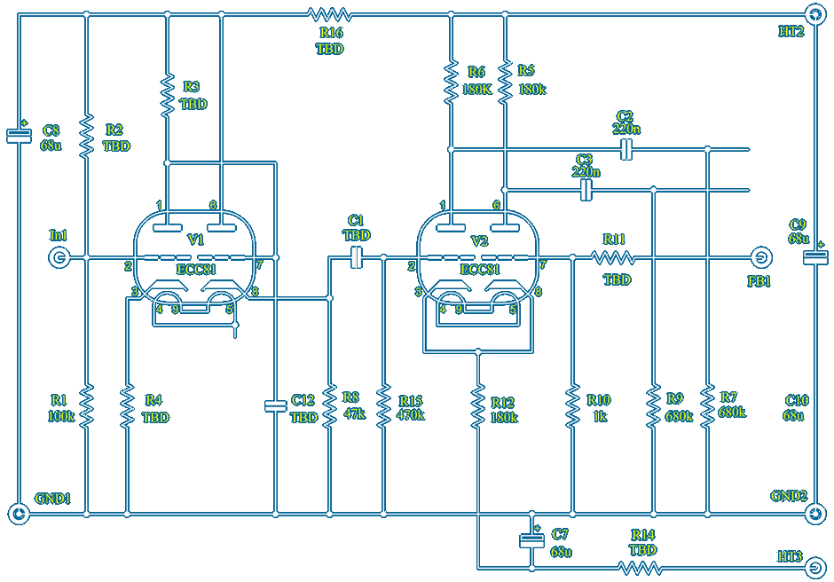
The circuit above uses a long tail or cathode coupled pair with the tail resistor R12 the same value as the load resistors R5 and R6 which are 180kΩ ~ R7 and R9 are 680kΩ which are the same values as the QUAD II circuit so the only difference in the two circuits from V2 anodes will be the internal anode resistance ra of each half of V2 Previously had I used only a long tail pair with various high mu triodes to try and simulate the single stage QUAD II driver design ~ So that negative feedback (NFB) from the output transformer can be directly applied to the long tailed pair non inverting input grid ~ both control grids (g1) ideally need to be referenced to 0V HT3 is a negative supply derived from a pair of silicon diodes in full wave rectifier across the HT winding ~ The positive HT via V5 and L1 is about 40V to 60V lower than the negative HT3 ~ R14 is chosen to position the anodes of V2 for maximum unclipped swing with minimum distortion while also providing additional smoothing with C7 I had also tried semiconductor current sources in place of R12 without a –Ve supply and current source loads for R5 and R6 but always more open loop gain was required even if only a small amount of overall NFB was to be applied and always the circuit was too complicated for little if any performance advantage ~ Welcome to triode µ With the values show above the anodes of V2 sit at about 170V and the gain from V2 input to each output was about 30x to 35x for various samples of ECC81 ~ When coupled to the KT66 g1's ≈1.2V to 1.4V is required for a 10W output ~ The overall gain from C1 input to speaker terminal output is about 6.5x and 1.7V is required for 15W output (11V across 8Ω or 15V across 15Ω) but this is before feedback is applied When fitted with ECC83s the gain is higher at ≈15x but no bias adjustments are required and it is this feature of the long tail pair with –ve supply and direct NFB that I liked ~ The circuit can be used with almost any pin compatible valves but some like ECC82 will require >5Vinput for 15W out and with NFB the input may need to be greater still The mutual conductance gm of triode valves increases with anode current Ia but the value of load resistors RL {R5 and R6} will need to be lowered to maintain the operating point ~ The internal anode resistance ra decreases with Ia and because it appears in parallel with RL the gain of a practical long tail pair amplifier may not be much higher As Ia increases ~ the increase in gm and the reduction in ra tend to 'level out' ~ as does the maximum possible gain µ available from a triode ~ There appears to be little advantage using high Ia in a triode voltage amplifier because the power dissipated in the valves and the load resistors increases greater than the gain Many triodes can become more linear as Ia increases and because ∆ra and ∆gm level out with ∆Ia the effect of dynamic changes also reduces The Triode Sound ~ To achieve maximum gain with high with Ia ~ current sources could be used for the loads but this adds yet more complexity to obtain a stable operating point The long tail pair circuit was modelled with PSPICE and some manual calculations were to done to establish how it would interface with the QUAD KT66 output stage but the only way to tell for sure was to build the circuit and fit it to a QUAD II in place of the EF86 driver and measure the open loop gain and frequency response etc. |
||||||
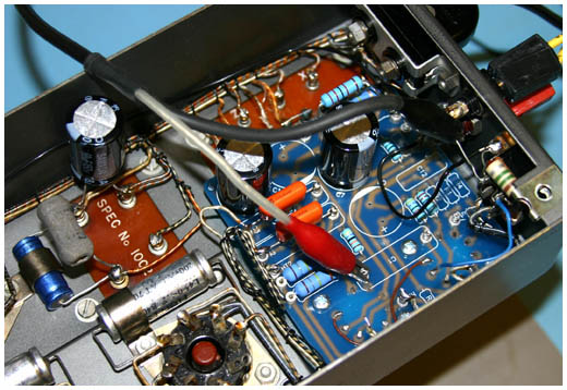 |
The circuit above was originally used for a Beard Audio amplifier modification but I also made the circuit on a PCB to fit neatly into the limited space in the QUAD II chassis
It is a single sided board with PCB mounted ceramic valve holders fitted on the solder side as used for my other valve project PCBs ~ I have seveal PCBs still available if you want to try the circuit Capacitors C1 ~ C2 ~ C3 are mounted on turret tags to enable different types to be easily changed without having to remove the PCB |
|||||
| In the picture above only the V2 components are fitted and the cathode coupled phase splitter driving the QUAD II KT66 output stage is being tested with an HP35670A FFT analyser for open loop THD ~ frequency response and stability with various ECC81s ~ ECC83s and E80CC etc.
It would appear that the QUAD II was designed for about 40dB or 100x open loop gain and for 20dB or 10x closed loop gain ~ The feedback is taken from point Q on the OPT which is at half the output voltage for the 15Ω tap and the 'amount of feedback' as traditionally calculated by 20Log(1+ßAo) is 20Log(1+0.175x50) = 19.8dB Applying more feedback to reduce Ao by 27dB can show signs of instability and this is typical of many valve amplifiers ~ The gain margin needs to be at least 6dB to allow for open circuit stability and not much more as Ao will not be large to start with ~ Beware of any audio amplifier that 'Must not be operated without a load' As marked on the schematic above the aim was to apply overall F.B. to the non inverting grid of V2 but the voltage gain of the output stage from each KT66 g1 to the 15Ω output is about 0.5x or –6dB so the 25dB gain from the long tailed pair phase splitter using ECC81 gave only 20dB of open loop gain requiring 100% F.B. by making R11 0Ω to achieve similar output impedance and performance to the QUAD circuit The long tailed pair phase splitter with negative supply will accept many different valves without bias changes and this was interesting because apart from slight gain variations there appears to be no difference in sound between ECC81s ECC82s and ECC83s so no good for a valve shootout ~ There is a sharper stereo image and possibly better control of transients so maybe triodes do have something that pentodes don't ~ In some configurations The input gain stage V1 is based on my amplifier/buffer gain block using an un–bypassed cathode resistor and positive raised g1 for the first valve but to achieve 20dB gain to drive the cathode coupled phase splitter I used the 'auto bias' value for R4 with R2 not fitted and adjusted R3 for 20dB gain and R16 for the operating point The reason the amplifier buffer configuration was chosen was it offers a predictable gain outside the phase splitter feedback loop which is simply determined by the ratio of R3 and R4 ~ The cathode follower ensures this gain is not affected by loading and its low output impedance ensures the Miller capacitance of the splitter is not a problem The driver performed well but the valve for V1 needs to be an ECC81 and different ECC81s showed that sometimes the third harmonic was higher than the second and although this was not apparent from listening it was something I wanted to avoid plus the primary source of distortion was from this first stage so back to . . . How does the QUAD II EF86 Driver work so well |
||||||
|
The additional large negative supply required for the cathode coupled phase splitter is not difficult to arrange but the original QUAD driver design was simpler and achieves about 46dB gain from input to each KT66 g1 with only 2 pentodes and a single HT well smoothed supply I had previously used triode cascodes in a cathode coupled phase splitter circuit with a 350V negative supply similar to the one above and also in the QUAD driver circuit topology which ~ along with a html version of Amplifiers and Superlatives ~ was the first 'content' for my original 1993 dc~daylight website |
 |
|||||
| The original QUAD II driver topology shown above can produce the maximum gain available from the first EF86 V1 as if it were in common cathode mode with a bypassed cathode resistor ~ despite the fact that R4+R10 is un–bypassed and therefore would appear to reduce the maximum gain of the first stage by about 3.5dB
|
||||||
 |
The schematic on the left is based on the QUAD II driver but configured as a simple 'floating paraphase' splitter by shorting R8 and fitting R8A ~ R7 and R9 now feed g1 of V2 with a signal which is the 'difference' between the outputs of V1 and V2 and as such the circuit is self balancing and often called as a see—saw phase splitter as described here
The common cathode resistors R4+R10 carry the equal and opposite signal currents of V1 and V2 and these cancel causing zero voltage change at the connected cathodes but they also reduce the gain by about 3.5dB so the maximum gain available from V1 is not achieved |
|||||
| A problem using the see–saw variant of the paraphase splitter as shown above is that R8A is required for the d.c. path to ground for the KT66 g1's as well as V2 g1 ~ R8A with R7 and R9 needs to be low enough such that the KT66 maximum grid bias resistance is not exceeded and high enough so as not to load the signal to V2 g1
The main problem is however when applying overall negative feedback from the output transformer ~ Negative feedback needs to be applied to V1 and not V2 or the circuit will be unstable ~ The feedback could be applied to g1 of V1 but not easily without lowering the input imedpance and the loading the 22 pre–amp If the feedback were applied to the junction R4 R10 without some circuit changes it would be negative feedback for V1 but positive for V2 ~ The change in the QUAD II design was to place a low value resistor R8 between R7 and R9 such that the signal across R8 was just enough to give V2 the same but opposite phase output as V1 The QUAD circuit is now similar to a regular paraphase design where the junction of R8 and R9 would be connected to signal ground and (R8+R7)/R8 would match the gain of V1 suggesting a gain of 48dB for each output ~ This allows for a lower resistance path for the KT66 g1's without undue loading on the splitter outputs The junction of R8 and R9 in the QUAD II is connected to the junction of R4 R10 and the feedback resistor R11 ~ The feedback signal is developed across R10 and the input to V2 across R8+R4 ~ R8 is 'floating' between R7 and R9 so any signal at the junction of R4 and R10 also appears at V2 g1 so V2 is not subject to positive or negative feedback The QUAD II driver is a simple cathode coupled paraphase phase splitter with additional a.c. coupling via C1 between the screen grids [ g2 ] of the EF86 pentodes which should be left as is ~ The clever bit is preventing positive feedback to V2 by positioning the junction of R8 and R9 at the feedback point and not to signal ground |
||||||
| The QUAD II driver is a 'single' stage of pentode gain ~ Triode drivers in their traditional form require 2 or more stages of gain in series or cascaded
An obvious choice to directly replace the pentodes in the QUAD design or other is a pair of cascaded triodes acting as a single valve in the configuration known as a cascode Cascodes using dual triodes like the ECC81 and ECC83 operated at Ia ≈1mA will give >46dB of gain using the same values for R5 R6 R7 and R9 as the QUAD circuit The schematic on the right is a variation of my 1992 cascode driver with the addition of R14 to balance the d.c. operating point of V2 and this time using ECC88s in place of the ECC81s |
 |
|||||
| In practice ECC81 ECC83 ECC85 and ECC88 and some other dual triode cascodes give a gain 47dB to 50dB in the QUAD II driver circuit with minimum changes other than R4 ~ The output resistance and thus open loop bandwidth reduction due to stray C is lowest with ECC88s which like ECC85s and 6BQ7A have the same heater connections as the EF86 so less rewiring
Building the cascode driver shown above using the original tag board is quite simple and makes for a much neater final product than some other triode mods ~ Note the top anode and bottom cathode of the cascode are the same pins as the EF86 but the wire between pins 3 and 8 of V1 and V2 have to be removed to join cathodes One problem with the cascode ~ especially when using an ECC88 ~ was despite using well balanced dual triodes there was often a large d.c. imbalance at the output anodes ~ This problem is also seen on a standard QUAD II using EF86s because the auto bias voltage for V1 is across R4+(R10||R11) and the bias for V2 is only across R4 Whether using cascode triodes or EF86s the imbalance can be compensated for by inserting a resistor R14= 2x(R10||R11) in series with V2 cathode ~ R14 also tends to linearise the V2 cascode but also lowers its open loop gain ~ The open loop balance of the outputs can be restored by increasing R8 to about 3k3Ω
I have made a double sided PCB with ground–plane for the cascode mod which has been fitted in my Majestic Mod QUAD IIs ~ In all my triode 'mods' I have tried to keep the anode loads and supplies around the valves similar to those of the EF86 circuit such that only the features intrinsic to the triodes are being evaluated With the E88CC cascode it is possible to use the original QUAD circuit topology with minimum changes ~ Lowering the anode load resistors to about 100kΩ and operating each valve at about 2mA gives a 'tighter' drive to the KT66 grids and lower overall phase shift to 100kHz and above ~ increasing the anode current beyond 2mA has little advantage because the load resistors R5 and R6 need to be further reduced to maintain the d.c. conditions |
||||||
 Note in the QUAD II circuit the d.c. path for the KT66 control grids through R7 and R9 is not directly connected to 0V ground but is via R10 in parallel with R11 and because the cathode currents of V1 and V2 pass through these resistors the KT66 grids will be at ≈200mV not 0V even with perfect
![]()


" I don't care what you do at home ~ Would you care to explain "