![[keith-snook.info]](/stuff/keith-info-S.png)

~ Op–Amp Class A Current Dumping output ? ~

The diagram opposite is part of the input section of the old but still excellent Tektronix AA501 audio analyser
One thing that interested me when I looked at putting 'better' op–amps in the circuit to get a lower noise floor was the way U1432 [ centre of picture ] was configured
The first edition of the AA501 manual shows a 68Ω resistor R1435 between U1432 pins 5 & 6 and my later model from 1984 had R1435 changed to 150Ω
The purpose of U1432 is to take the balanced input signal amplified by U1420A/B and provide a low noise low distortion low output impedance unbalanced 1.5x larger signal to the various function stages throughout the analyser ~ The AA501 noise was already lower than –115dBm B22.4 [1.4µV] so no op–amps were changed
So what is the purpose of the resistor R1435 which had its value changed for later AA501 models ?
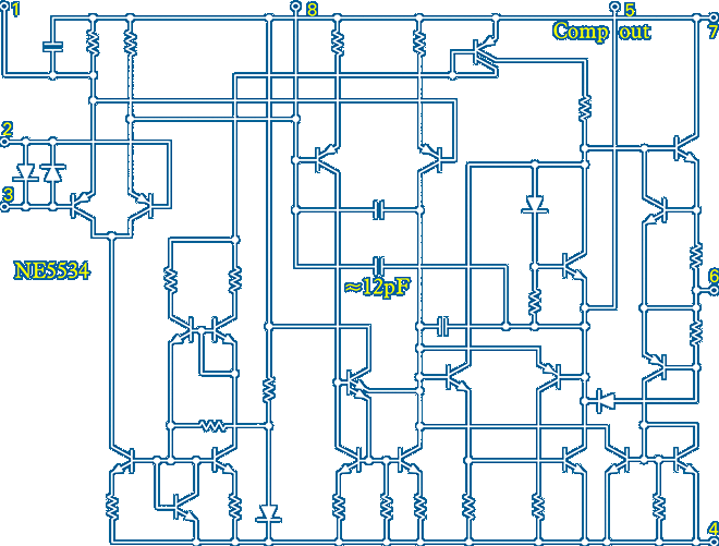
As seen in this incorrect schematic from Philips Pin 5 of the NE5534 and some other op–amps like the AD744 is marked as a compensation pin and is an output capable of driving a capacitive load back to Pin 8
Pin 5 is an internal buffered node which would appear to be a class A drive point for the output transistors which are likely operating in class AB

Modelling the AA501 input with and without R1435 in place proved inconclusive but did indicate that the Spice models most manufacturers provide have a lower than practical output impedance at Pin 5
U1432 in the AA501 has its gain set at x1.5 [<10dB] so has external compensation C1424 and C1522 applied in the traditional way and not using the NE5534A Pins 1 and 8
To check a modelled NE5534 against the real thing I built a breadboard circuit with 20dB gain and links for resistors and capacitors from Pin 5 and a link to put 22nF across the 2kΩ load on the output ~ Click the picture
Testing the real circuit with 68Ω to 150Ω across Pins 5 and 6 in and out of circuit and loading the output with 22nF using the 0.1" link led to the conclusion that the resistor R1435 in the AA501 was providing feedforward compensation to the output allowing the NE5534A to drive a capacitive load up to 300kHz with low distortion

Tests were done with a 35670A FFT analyser using periodic chirp source and uniform window to show instant wide range frequency responses with the output also monitored on an analogue oscilloscope via a TEK AA501 to catch any odd behaviour ~ AD744s were also evaluated and overall gave better results driving 22nF than several different makes of NE5534A
The worst results driving the excessive 22nF load were with some 1981 Signetics NE5534A which required extra external compensation capacitor and even then tended to oscillate when near to clipping as can be seen pictured where the negative half cycle trace has 'widened' ~ The bursts synchronised on the second trace at 320kHz are via the AA501 to remove the 1kHz fundamental and are on a different scale
It is likely that NE5534s made by different companies over a 44 year period had differing values of internal compensation C which would have taken a relatively large area of silicon and in older parts may well be damaged ~ There also appears to be a variation in the on chip resistor values used by each manufacturer
In the early eighties we were presented with the compact disk and a promise that they would last forever but now 40 years later we have CDs failing due to the aluminium oxidising but a 50 year old vinyl copy of Dark Side of the Moon plays well ~ Their Silicon is probably still okay but many op–amps have thin metal capacitor plates
I used the term feed–forward to describe the signal that R1435 passes to the output to give a current in parallel with that of the output devices and it follows that I believe the region around the zero crossover is now actually class A and that R1435 current is always present although reduces as the signal excursions away from zero
I also proposed that the QUAD 405 is a feed–forward amplifier with the output devices not biased class B or AB like these op–amps ~ This caused some argument on a few audio forums and I too have to admit that the original 405 design has 2 'crossover' regions but they are not at signal zero crossing or near output device zero current

Looking closely at the picture of the op–amp breadboard you will see it resembles the schematic shown here with C8 and L2 and 22nF which can be switched using 0.1" links
Because the NE5534 Pin 5 is a class A output the circuit now resembles the QUAD 405 current dumping topology where the main output follows the Class A stage output when L2 ÷ R38 = C8 x R20 ⁄⁄ R21
With the compensation capacitor C8 connected to pin 2 there is still a second Miller capacitor of ≈12pF inside the NE5534 across Pins 5 and 8 which makes the circuit topology not exactly current dumping ~ Measurements were made with a variable 10pF-100pF C8 connected to Pin 2 and also to Pin 8 in parallel with the internal Ccomp
With C8 connected from Pin 5 to Pin 8 and adjusted to 'balance the bridge' the circuit is more like the QUAD405 circuit with C8 connected to the collector of Tr2 and not at the emitter as in my mods ~ If the circuit could be made with an op–amp like the NE5534 but without any internal compensation perhaps this configuration may prove useful ?
 I am not proposing that a suitable op-amp connected in the current dumping topology gives any audio improvement over the same op-amp used as shown in its data sheet but the R1435 feed–forward technique used by Tektronix in the AA501 does improve distortion of its NE5534
especially when driving a capacitive load
I am not proposing that a suitable op-amp connected in the current dumping topology gives any audio improvement over the same op-amp used as shown in its data sheet but the R1435 feed–forward technique used by Tektronix in the AA501 does improve distortion of its NE5534
especially when driving a capacitive load
Nowadays you don't see internal schematics like those of the NE5534 but you may see basic diagrams with "distortion cancelling circuit" in a box ~ Burr Brown had patented such circuits but were bought buy Texas Instruments [TI] who also have/had the LME range of op-amps which may use internal Class A feedforward to reduce distortion but how they make op-amps with better Bass response is always going to remain a secret
![]()


" Agents of the Law luckless pedestrian ~ I know your out there with rage in your eyes and your megaphones "